Why is an ionizer required in the i-line region of semiconductor manufacturing? To understand this, we need to explore the following four dimensions:
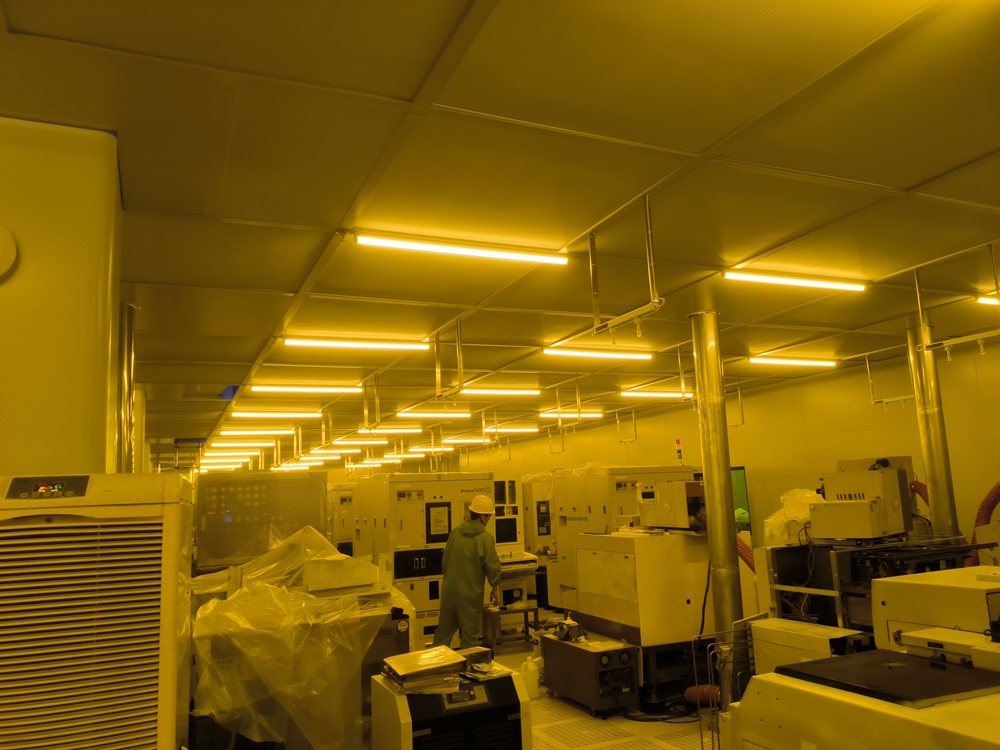
The i-Line region is a dedicated cleanroom area for semiconductor photolithography. Its primary function is to accurately transfer circuit patterns from the photomask onto the photoresist on silicon wafers. Its environmental requirements are far stricter than standard cleanrooms, with key characteristics including:

Light Environment Control: Yellow light (wavelength 500–600 nm) is used instead of white light because photoresists, especially positive photoresists, are sensitive to short-wavelength visible light such as blue and violet. White light can cause premature exposure, while yellow light does not trigger the photoresist reaction, hence the term "yellow light region".
Ultra-High Cleanliness: Class 1 or higher (≤1 particle ≥0.5 μm per cubic foot of air). Even microscopic particles adhering to wafers or photomasks can cause pattern defects, such as line-width deviations or open circuits.
High-Density Precision Equipment: The area contains photolithography machines (core equipment worth tens of millions of RMB), photomasks (high-precision quartz substrates storing circuit patterns at a very high cost), and silicon wafers, all of which have extremely low tolerance for physical or chemical interference.
Damage to Devices: Electrostatic discharge (ESD) can break down the wafer oxide layer, ablate the mask's chromium layer, or damage photolithography sensors, directly causing high-value device failure.
Environmental Contamination: Static electricity attracts airborne particles, which adhere to wafers or masks, causing missing or broken patterns that are only detected in later stages, drastically reducing yield.
Process Interference: Static can lead to uneven photoresist coating, rough development edges, and misalignment between masks and wafers. With overlay accuracy requirements ≤1 nm, even tiny deviations can fail.
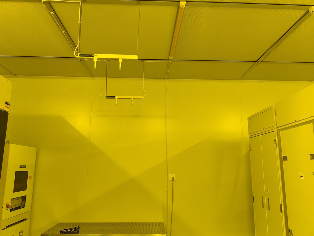
Neutralize Static Charges and Prevent ESD: Ionizers generate balanced positive and negative ions, delivering them via clean airflow compatible with the i-Line cleanroom standards. This keeps surface potentials within ±10 V, far below the ESD threshold, effectively preventing discharges.
Suppress Particle Adhesion and Maintain Cleanliness: By neutralizing static on surfaces and in the environment, ionizers eliminate electrostatic attraction, preventing particles in the air from adhering to wafers and masks.
Ensure Process Accuracy and Stabilize Yield: With electrostatic control, photoresist coatings are more uniform, development reactions are more stable, and mask-to-wafer alignment is more precise, safeguarding overlay accuracy.

Not all ionizer static eliminators are suitable for the i-Line region. Devices must meet these specific requirements:
No Particle Contamination: Ionizer components must be made of low-dust materials, and ion generation elements (e.g., needle electrodes) must be regularly cleaned.
No Chemical Contamination: Airflow must be treated to remove moisture and oil to avoid contaminating photoresist or masks.
No Light Interference: Ionizer housings and indicators must be made of materials that block visible light to prevent inadvertent exposure.
Real-Time Monitoring: Paired with electrostatic potential monitors and sensors, ionizers must provide real-time feedback. Alarms trigger if surface potentials exceed safe limits.
As the "core battlefield" of semiconductor photolithography, the i-Line region's nanoscale process accuracy, high-value devices, and ultra-clean environment make static electricity a critical hazard. QEEPO ionizers, through ion neutralization, address this challenge from three dimensions: preventing ESD damage, suppressing particle adhesion, and ensuring process accuracy, making them essential equipment for stable yield in semiconductor manufacturing.