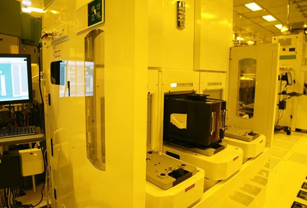
In semiconductor wafer manufacturing, the EFEM (Equipment Front End Module) serves as the "bridge" connecting the AMHS (Automated Material Handling System) and process equipment (such as lithography, etch, or deposition tools). It is responsible for FOUP (Front Opening Unified Pod) docking, wafer transfer (e.g., from FOUP to the process tool's wafer stage), and represents a critical step where wafers are exposed to the ambient environment. EFEM is also a high-risk area for electrostatic discharge (ESD).
An EFEM typically consists of a FOUP Load Port, wafer handling robot, internal clean chamber, ionization system, electrostatic monitoring unit, and control system. Each component has precise electrostatic control requirements and design specifications, as detailed below:

The Load Port is the first point of contact for the FOUP entering the EFEM. It must simultaneously achieve sealed docking and static dissipation. Key requirements include:
Material and grounding requirements:
The docking surface (where the FOUP contacts the Load Port) must use conductive engineering plastics (e.g., carbon fiber-reinforced PEEK, surface resistivity 10⁶–10⁹ Ω) or nickel-plated metal to prevent static buildup from friction.
The platform must connect to the EFEM main ground via elastic grounding contacts, with grounding resistance ≤1 Ω.
FOUP locating pins (used for securing the FOUP) must be metal and directly grounded to ensure that after placement, the FOUP shell is electrically connected to the EFEM ground network, with surface potential ≤ ±50 V (measured after 5 seconds of resting).
Cover opening mechanism control:
The FOUP cover must open via translational motion rather than rotational (rotation generates frictional static). Opening speed ≤50 mm/s to minimize friction.
Grippers must be covered with anti-static rubber (volume resistivity 10⁶–10⁸ Ω) to prevent charge generation from metal-plastic contact.
Advanced Load Ports may integrate miniature electrostatic sensors to detect FOUP surface potential before opening. If potential exceeds ±100 V, an alarm is triggered, and opening is prohibited.
As the only EFEM component that directly contacts wafers, the robot's micron-level motion precision is inseparable from a comprehensive electrostatic control strategy, ensuring that all stringent ESD requirements are strictly met.
Material selection (core criteria):
The robot body, especially the End Effector, must use electrostatic dissipative materials.
Motion and grounding control:
Speed must be staged: wafer pick-and-place ≤30 mm/s, translational motion ≤100 mm/s; acceleration ≤500 mm/s². This reduces air friction and inertial friction.
The robot must employ multi-path grounding (e.g., conductive bearings at joints, base connected to EFEM main ground) to ensure all parts have grounding resistance ≤0.5 Ω, with continuous real-time monitoring via built-in current sensors.
Wafer contact protection:
End Effector contact area ≥20% of wafer area to avoid localized charge concentration; contact pressure ≤50 g to prevent deformation and friction.
Some high-end EFEMs apply anti-stick coatings on the End Effector to reduce frictional adhesion with wafers.
The EFEM chamber provides a sealed, clean environment (typically Class 1–Class 10), requiring control of spatial static charge and particle adhesion. Manufacturers rely on specialized static control instruments to continuously validate environmental stability and minimize the risk of particle attraction caused by uncontrolled surface charges.
Chamber material and structure:
Internal walls must be conductive stainless steel (316L, electro-polished) with surface resistance ≤10⁶ Ω. All joints must be sealed with conductive adhesive, ensuring full chamber grounding to form a Faraday cage, isolating external electric fields.
No sharp structures (e.g., protruding screws, unpolished edges) are allowed to prevent corona discharge.
Airflow and humidity control:
Airflow: 0.2–0.4 m/s to balance particle removal and avoid friction-induced charging; airflow passes through electrostatic-dissipative HEPA/ULPA filters, with grounded frames.
Humidity: stable at 45–55% (±5%). Humidity <40% increases static buildup; >60% risks wafer oxidation or condensation inside the chamber.
Ionization is key for controlling wafer and chamber surface charges, requiring fast, precise, and contamination-free operation.
Ion source selection:
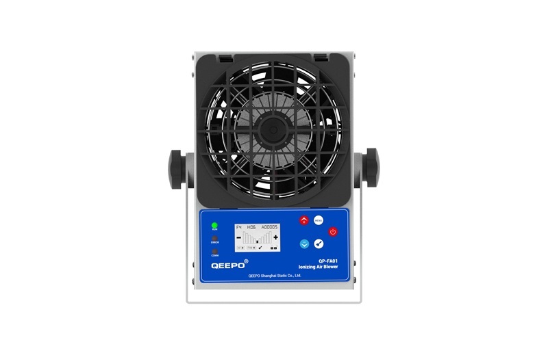
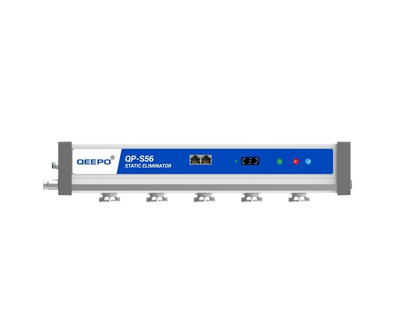
Recommended: QEEPO ionization fans or QP-S56 ion bars, instead of unipolar sources, which may cause charge accumulation.
Fans should be installed at the top of the EFEM chamber (covering the robot motion area), with at least two units to avoid neutralization dead zones.


Key technical metrics:
Ion balance: ≤ ±10 V (measured 300 mm from the source along wafer path)
Neutralization time: ≤1 s (to reduce 1000 V to ±30 V)
Oil-free and particle-free operation: Use oil-free compressed air or clean nitrogen to drive the ionizer.
Dynamic adjustment:
Ion system must integrate with EFEM control: speed increases when robot moves, decreases when wafer is stationary, to minimize airflow disturbance.
High-end EFEMs may integrate ion concentration sensors; insufficient ion density triggers alarms and backup ion sources.
EFEM must monitor ESD conditions in real time using QP-C01 sensors for traceable risk control.
Monitoring point layout:
Mandatory: FOUP surface at Load Port, End Effector, midpoint of wafer transfer path, internal chamber space
Optional: process tool interface, ion fan outlet
Sensor specifications:
Type: non-contact electrostatic potential sensor
Range: -2000 V to +2000 V
Accuracy: ±1%
Sampling frequency: ≥10 Hz
Alarm and interlock:
Two-level thresholds:
Warning: ±50 V → trigger ion system boost, production continues
Shutdown: ±100 V → stop robot, close Load Port, prevent wafer damage
Alarm data must be uploaded to MES in real-time, recording time, location, potential for yield analysis, and traceability.
EFEM electrostatic control involves materials, design, monitoring, and maintenance. Its core goal is to reduce wafer electrostatic risk during transfer to zero-damage.